
§6 What is the Working Principle of Solid-State Relays
Because of the different application environments, solid-state relays have slightly different internal components, but the working principle is similar. The internal equivalent circuit diagram of ordinary solid-state relays is shown in the figure below (Figure 6.1). The principle of solid-state relays can be simply described as: for the NO-SSR, when the appropriate control signal is applied to the Input Terminal (IN) of the solid-state relay, the Output Terminal (OUT) will be switched from the off state to the on state; if the control signal is cancelled, the Output Terminal (OUT) will be restored to the off-state. In this process, the solid state relays realize non-contact control of switch states of the load power supply which is connected to output terminals. It should be noted that the input terminal can only be connected to the control signal, and the load should only be connected to the output circuit.
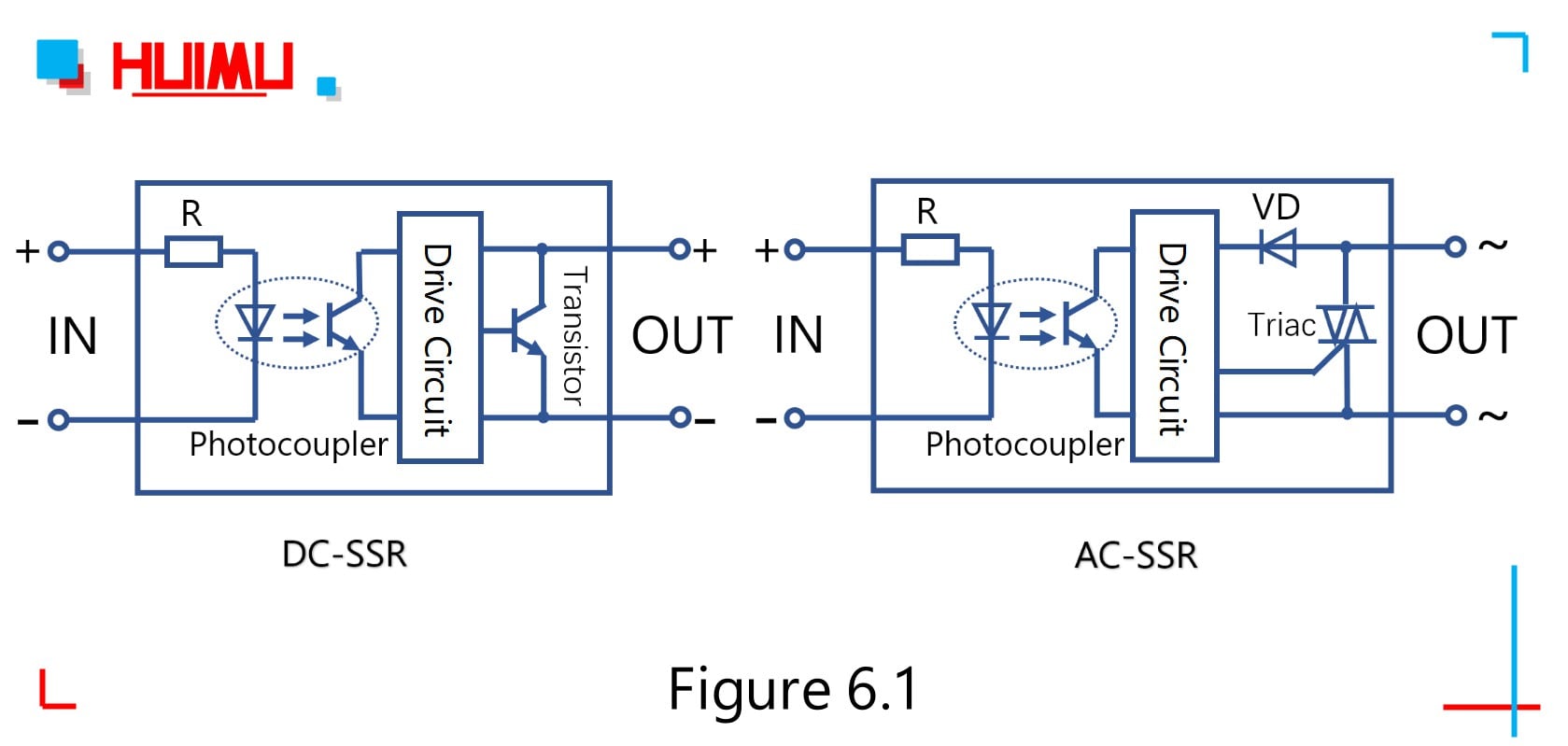
According to the type of load, SSR can be divided into two types: DC Solid State Relay (DC-SSR) and AC Solid State Relay (AC-SSR). The DC-SSRs act as a load switch on the DC power supplies, and the AC-SSRs act as a load switch on the AC power supplies. They are not compatible with each other and cannot be mixed.
1) DC solid state relay (Figure 6.1, Left), whose control signal voltage is inputted from the Input Terminal (IN), and then the control signal is coupled to the receiving circuit through the photocoupler, and eventually the signal is amplified by the amplifier to drive the switching state of the Transistor. Obviously, the Output Terminal (OUT) of the DC solid state relay is divided into Positive Terminal (+ pole) and Negative Terminal (- pole), be careful not to make mistakes when connecting the output terminal of DC SSR relay to the controlled circuit.
2) AC solid state relay (Figure 6.1, Right), is used to control the ON/OFF state of the AC load circuit. Unlike DC solid-state relays, the AC SSR relays use the bidirectional thyristor (Triac) or other AC electronic switching components. Therefore, there is no Positive/Negative Terminal in the Output Terminal (OUT) of the AC solid state relay.
The working principle of Zero-Crossing AC Solid-State Relays
Since zero-crossing AC solid state relays are completer and more typical than other types of solid state relays, the operation details of AC zero-crossing SSR relays can help illustrate the complete working principle of SSR relays:
1. The Function of Each Parts:
Following is the representation of the AC zero-crossing SSR (Figure 6.2). And the A~E circuit in the block diagram forms the body of the Zero-Crossing AC SSR. On the whole, the SSR relay is a four-terminal load switch, with only two input terminals (③ and ④) and two output terminals (①and ②). When the AC Zero-Crossing SSR relay is working, as long as a certain control signal is added to ③ and ④ terminals, the ON/OFF state of the loop that between the ① and ② terminals can be controlled.
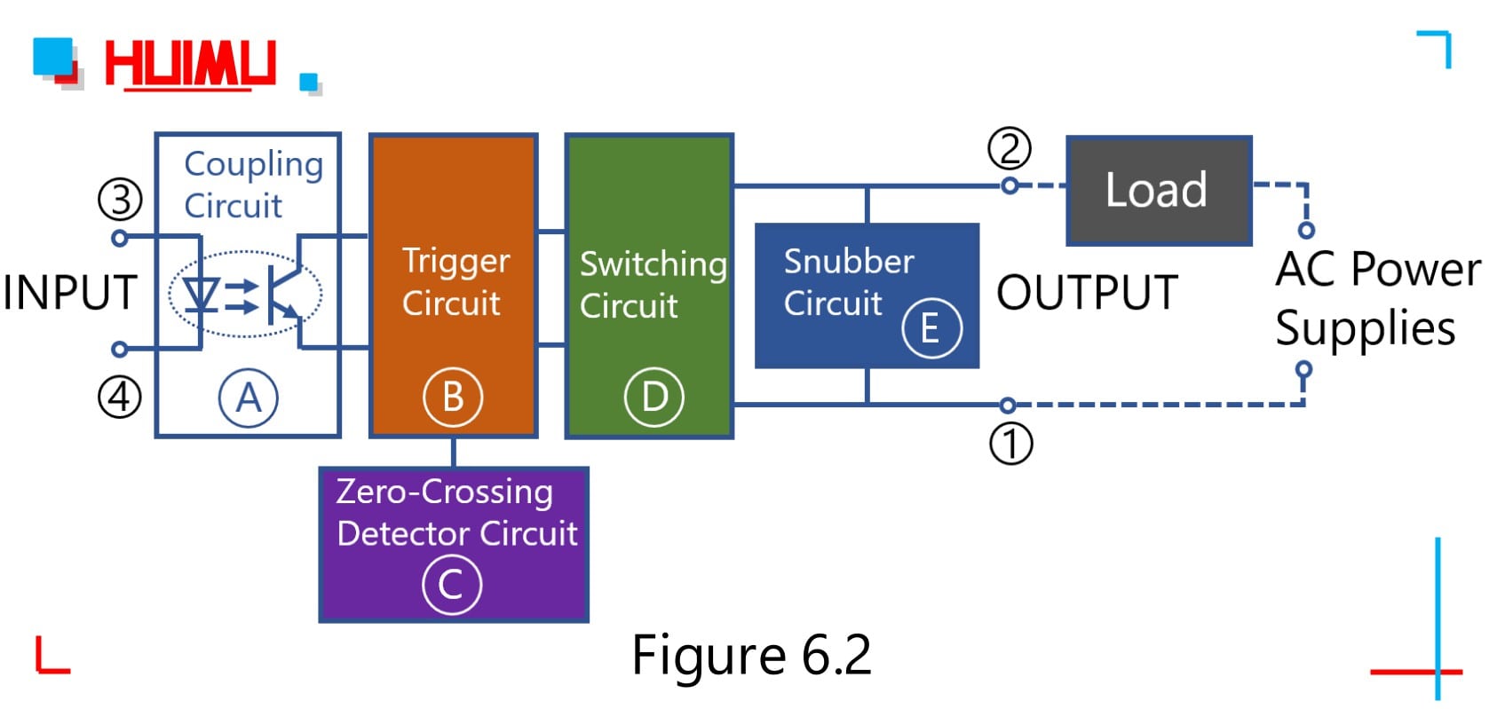
The Coupling Circuit A is used to provide an I/O channel for the control device that connected to the ③ and ④ terminals, and electrically cut off the connection between the input terminals and output terminals of the SSR to prevent the output circuit from interfering with the input circuit. The most commonly used component in the coupling circuit is the optocoupler with high action sensitivity, high response speed, and high dielectric strength (withstand voltage) between the input and output terminals. Since the input load of the photo-coupler is a light emitting diode (LED), this makes the input value of the solid-state relay easy to match the input signal level of the control device, and make it possible to connect the input terminals of the SSR relays directly to the computer output interface, that is, the solid state relay can be controlled by the logic level of “1” and “0”.
The function of the Trigger Circuit B is to generate a suitable trigger signal to drive the Switching Circuit D to operate. However, if no special control circuit is added, the switching circuit will generate Radio Frequency Interference (RFI), which will pollute the grid by the higher harmonics and the spikes, so the Zero-Crossing Detector Circuit C is specifically designed to solve this problem.
The Snubber Circuit E is designed to prevent spikes and surges from the power supply from causing impacts and disturbances (even malfunctions) to the switching transistors. Generally, an RC circuit (resistor–capacitor circuit, or RC filter or RC network) or a non-linear resistor (such as varistor) is used as the snubber circuit. The varistor, also called voltage-dependent resistor (VDR), is an electronic component whose resistance value varies nonlinearly with the applied voltage, and the most common type of varistor is the metal-oxide varistor (MOV), such zinc oxide nonlinear resistor (ZNR).
2. The Function of Each Components:
The figure below is the internal schematic diagrams of the zero-crossing trigger type AC-SSR (Figure 6.3)
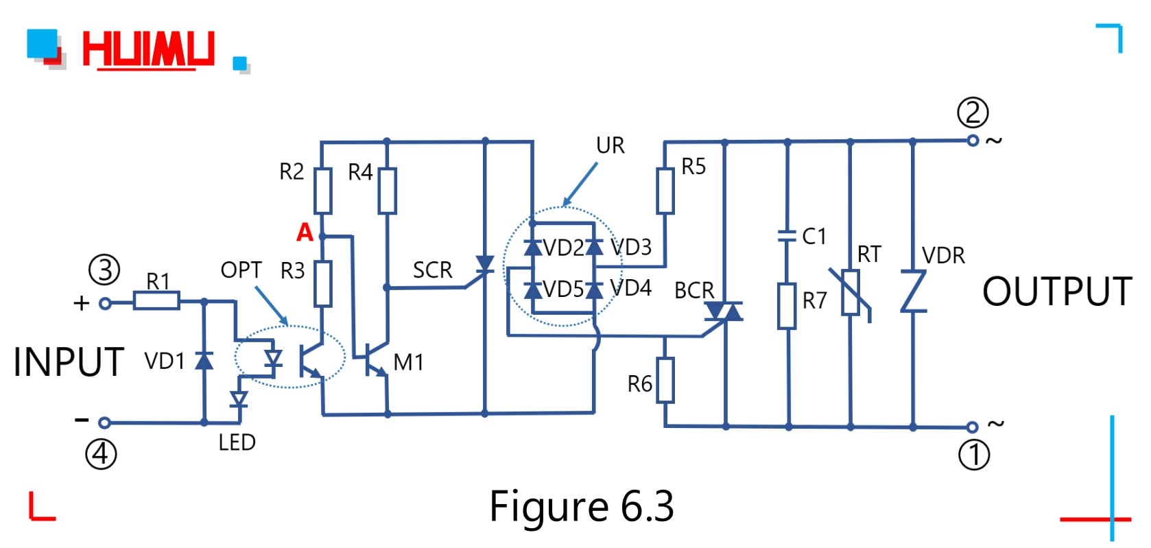
R1 is a current limiting resistor that limits the input signal current and ensures that the optocoupler is not damaged. LED is used to display the input state of the input control signal. The diodeVD1 is used to prevent the optocoupler from being damaged when the positiveand negative poles of the input signal are inverted. The optocoupler OPT electrically isolates the input and output circuits. The triode M1 acts as an inverter, and constitute the zero-crossing detection circuit with the thyristor SCR at the same time, and the operating state of the SCR thyristor is determined by the alternating-voltage zero-detection transistor M1. VD2~VD4 form the full-wave rectifier bridge (or full-wave diode bridge) UR. A bidirectional trigger pulse for turning on the triac BCR can be obtained from SCR and UR. R6 is a shunt resistor used to protect the BCR. R7 and C1 make up a surge absorbing network to absorb spike voltage or surge current in the power mains to prevent shock or interference to the switching circuit. RT is a thermistor that acts as an overheating protector to prevent solid state relays from being damaged due to excessive temperatures. VDR is a varistor that acts as a voltage-limiting device that clamp the voltage and absorbs excess current to protect the solid-state relay when the output circuit is overvoltage.
3. The Process of Working:
The AC zero-crossing solid state relay has the characteristics of being turned on when the voltage crosses zero and being turned off when the load current crosses zero.
When the opto-coupler OPT is turned off (i.e. the control terminal of OPT has no input signal), M1 is saturated and turned on by obtaining the base current from R2, and as a result, the gate trigger voltage (UGT) of the thyristor SCR is clamped to a low potential and turned off. Consequently, the triac BCR is in the off state because there is no trigger pulse on the gate control terminal R6.
When an input control signal applied on the input terminal of the solid-state relay, the phototransistor OPT is turned on (i.e. the control terminal of the OPT has an input signal). After the power mains’ voltage is voltage-divided by R2 and R3, if the voltage at point A is larger than the zero-crossing voltage of M1 (i.e. VA>VBE1), M1 will be in the saturated conduction state, and both SCR and BCR thyristors will be in the off state. If the voltage at point A is less than the zero-crossing voltage of M1 (i.e. VA<VBE1), M1 will be in the cut-off state, and the SCR will be triggered to conduct, and then the trigger pulse from “R5→UR→SCR→UR→R6” direction (or the opposite direction) is obtained on the control pole of the BCR to activate the BCR, and finally the load will be connected to AC mains.
Through the above process, it can be understood that M1 is used as an AC voltage detector for turning on the solid-state relay when the load voltage crosses zero and turning off the solid state relay when the load current crosses zero. And on account of the function of the zero-crossing detector, the impact of the load circuit on the load is correspondingly reduced, and the radio frequency interference generated in the control loop is also greatly reduced.
4. The Definition of Zero-Crossing:
Here it need be explained what is the zero crossing. In the alternating current, the zero-crossing is the instantaneous point at which there is no voltage present, that is, the junction between the positive half cycle and the negative half cycle of the AC waveform. In each cycle of alternating current, there will usually be two zero crossings. And if the power mains switches at the instant point of zero crossing, no electrical interference will be generated. The AC solid-state relay (equipped with a zero-crossing control circuit) will be in the ON state when the input terminal is connected to the control signal and the output AC voltage crosses zero; conversely, when the control signal is turned off, the SSR be in the OFF state until the next zero crossing.
In addition, it should be pointed out that the zero crossing of solid state relay does not actually mean zero volts of the power supply voltage waveform. Figure 6.5 is a section of the AC voltage sine wave. According to the characteristics of the AC switching component, the AC voltage in the figure is divided into three regions that correspond to three states of the SSR’s output circuit. And U1 and U2 respectively represents the threshold voltage and the saturation voltage of the switching component.
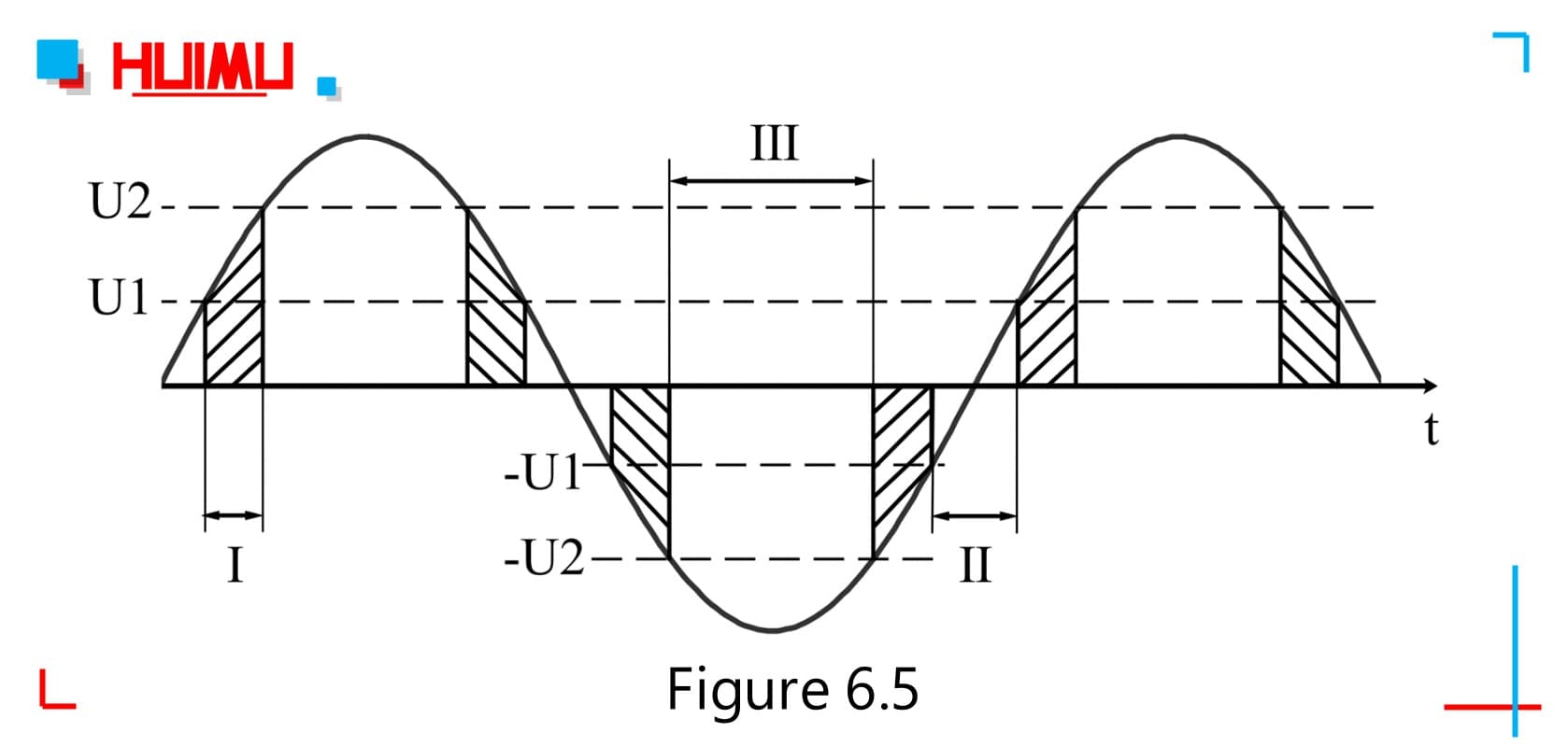
1) Region Ⅰ is the Dead Region (Cut-Off Region, Cut Out Region, or Turn Off Region), with an absolute value of voltage range of 0~U1. And in this zone, the SSR switch cannot be turned on, even if an input signal is added.
2) Region Ⅱ is the Response Region (Active Region, Cut-On Region, Cut In Region, or Turn On Region) with an absolute value of voltage range of U1~U2. In this zone, the SSR is immediately turned on, as soon as the input signal is added, and the output voltage increases as the supply voltage increases.
3) Region Ⅲ is the Suppression Region (Saturation Region) with an absolute value of voltage range greater than U2. In this region, the switching element (thyristor) is in the saturated state. And the output voltage of the solid-state relay will no longer increases with the increase of the power supply voltage, but the current increases with increasing voltage, which can be regarded as an internal short circuit state of the output circuit of the solid-state relay, that is, the solid-state relay is in the Switch-On state as an electronic switch.
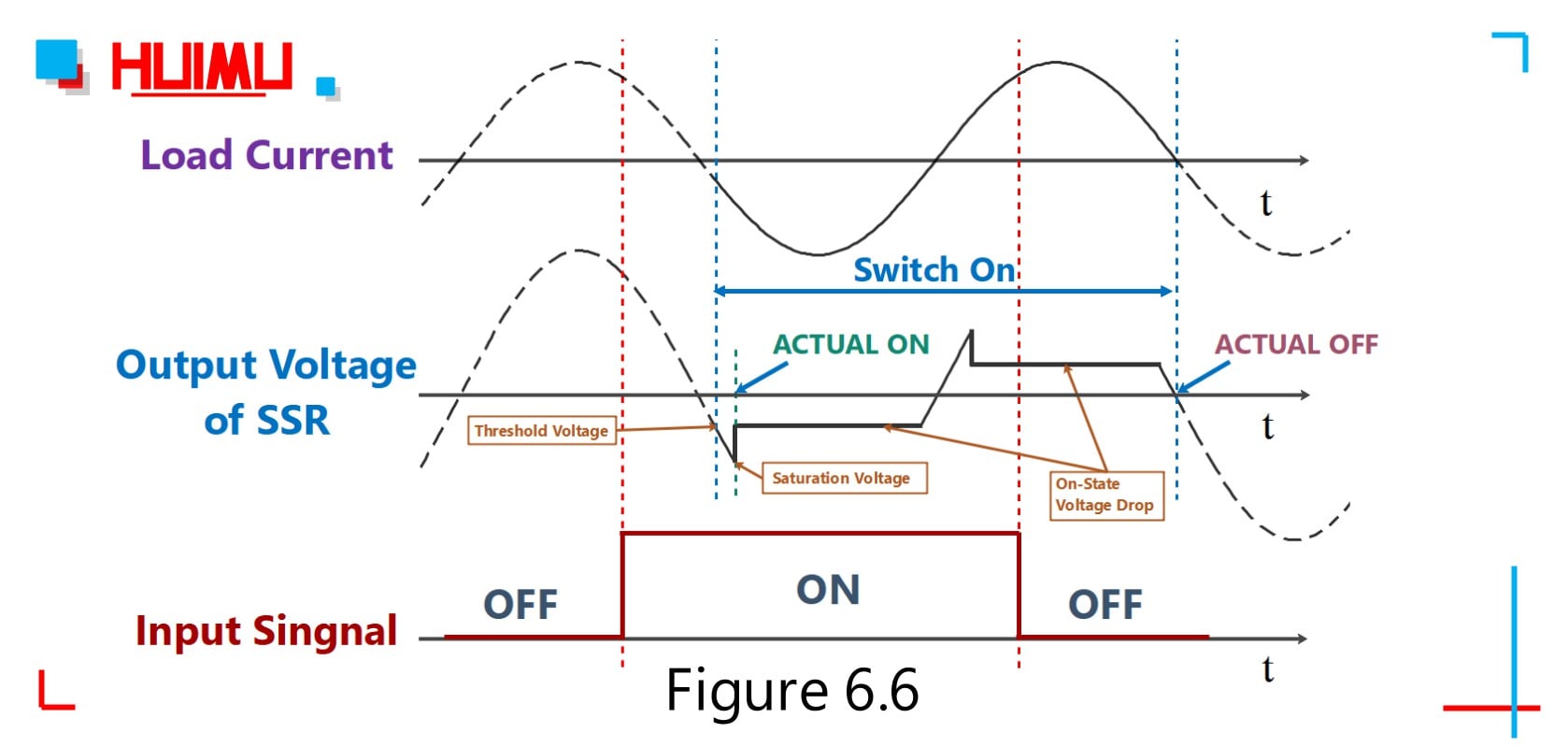
Figure 6.6 shows the I/O waveform of the zero-crossing solid-state relay. And because of the nature of the thyristor, the solid-state relay will be in the on state after the voltage of the output terminals reaching the threshold voltage (or the trigger voltage of the trigger circuit). Then the solid-state relay will be in the actual on state after reaching the saturation voltage, and at the same time, generate a very low on-state voltage drop. If the input signal is turned off, the solid-state relay will be switched off when the load current drops below the thyristor’s holding current or the next AC commutation point (i.e. the first time the load current passes through zero after the SSR relay turned off).
